Learn to decode a mobile chip with 4 real chips
You do not have to remember lakhs of codes. You only have to read every chip in the same four steps. Pick a real chip below and press Play.
The four steps
- Find the company. Look for the logo or name, for example SK hynix.
- Read the first letters. They tell you the type: eMMC, eMCP, UFS or uMCP.
- Find the capacity. One letter or two digits in the code give the GB.
- Ignore the rest. Variant letters, the second line and the date are not the GB.
Watch it on real chips
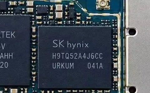
Code on the chip
URKUM 041A
- Find the company
The logo says SK hynix, so we use the SK hynix rules.
- Read the first letters
H9TQ at the start means eMCP: storage and RAM together in one chip.
- Find the capacity
The two digits after H9TQ are 52. In the SK hynix list, 52 means 64 GB.
- Ignore the rest
A4J6CC is the variant. URKUM is the end of the code and 041A is the date. None of these is the GB.
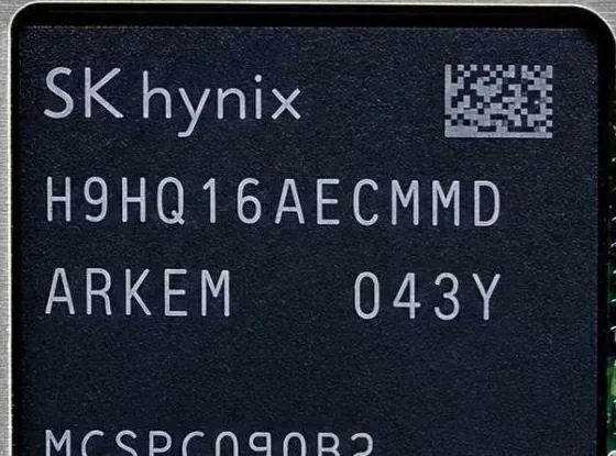
Code on the chip
ARKEM 043Y
- Find the company
The logo says SK hynix.
- Read the first letters
H9HQ means uMCP: UFS storage and RAM together in one chip.
- Find the capacity
The two digits after H9HQ are 16. In the SK hynix list, 16 means 128 GB.
- Ignore the rest
AECMMD is the variant. ARKEM finishes the code, so the full code is H9HQ16AECMMDAR-KEM. 043Y is the date.
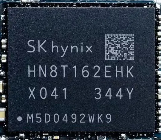
Code on the chip
X041 344Y
- Find the company
The logo says SK hynix.
- Read the first letters
HN8 means UFS: fast storage only, with no RAM inside.
- Find the capacity
After HN8 comes a letter and a digit: T1. In the HN8 list, T0 is 128 GB, T1 is 256 GB and T2 is 512 GB. So this chip is 256 GB.
- Ignore the rest
62EHK is the variant. X041 finishes the code (HN8T162EHKX041) and 344Y is the date. Careful: one digit, T0 or T1, doubles the GB.
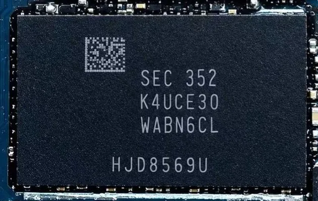
Code on the chip
HJD8569U
- Find the company
There is no SK hynix logo. The first line starts with SEC, which is Samsung's marking. So this is a Samsung chip.
- Read the first letters
The code starts with K4. Samsung K4 chips are RAM, not storage.
- Find the capacity
A RAM chip has no storage GB to read here. This is the RAM part of the board, not the part that decides its storage.
- Look for the storage chip
The storage chip is the other one: in this photo, the SK hynix HN8 chip above it. Always find the storage chip first.
Why the code and the photo look different
Makers print the code over two or three lines. Join the lines before you compare. On chip 2, the lines H9HQ16AECMMD and ARKEM together make H9HQ16AECMMDAR-KEM, which is the code stored in the database.
Practise next
- Learn the Samsung letter ladder and take the quiz.
- Read the rules for every maker in how to find the GB from a chip code.
Check a chip in one scan
Do not want to decode by hand? ChipGB Scanner reads the code and shows the GB, company and type in one scan.
Download for AndroidQuestions
Can I decode every chip like this?
Only the families whose rule is known. For other codes, such as Micron's five-character codes, you need a database or the app.
Why did chip 3 say T1 and not T0?
In the SK hynix HN8 list, T0 is 128 GB, T1 is 256 GB and T2 is 512 GB. One digit changes the GB, so read it slowly.
Is a Samsung K4 chip storage?
No. K4 chips are RAM. Look for the storage chip next to it.
This guide is general. Numbering rules differ by family, and some codes are exceptions. Confirm the GB with a verified source before you pay.